
Top China Manufacturer of High-Quality Surface Mount PCB Solutions
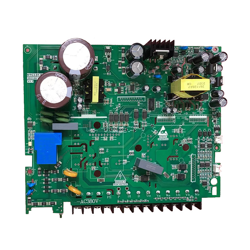
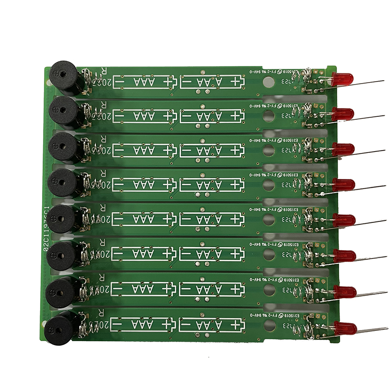
As a leading manufacturer of Surface Mount PCBs in China, I understand the importance of quality and reliability in every component. Our Surface Mount PCBs are designed with precision to meet the demanding standards of various industries. We’ve adopted advanced technologies and materials to ensure optimal performance and durability. I always prioritize customer needs, providing tailored solutions that fit unique specifications. Whether you require small batches or large-scale production, my team is dedicated to delivering on time while maintaining competitive pricing. Choosing us means partnering with a manufacturer who values innovation and quality. With years of experience in the field, we have established a reputation for excellence, making us a trusted choice for B2B purchasers. Let’s work together to elevate your products with our state-of-the-art Surface Mount PCBs!
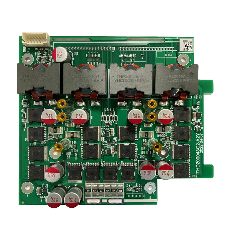
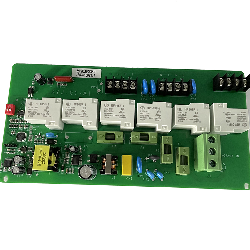


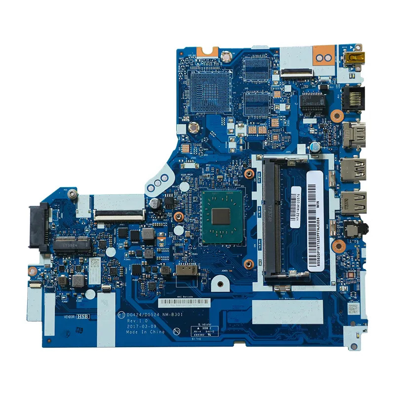
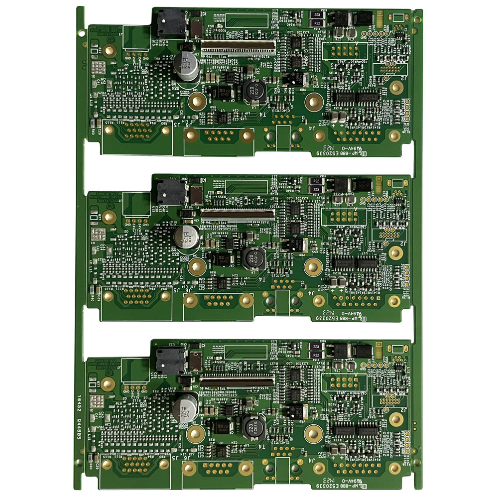
Surface Mount Pcb Application From Concept to Delivery
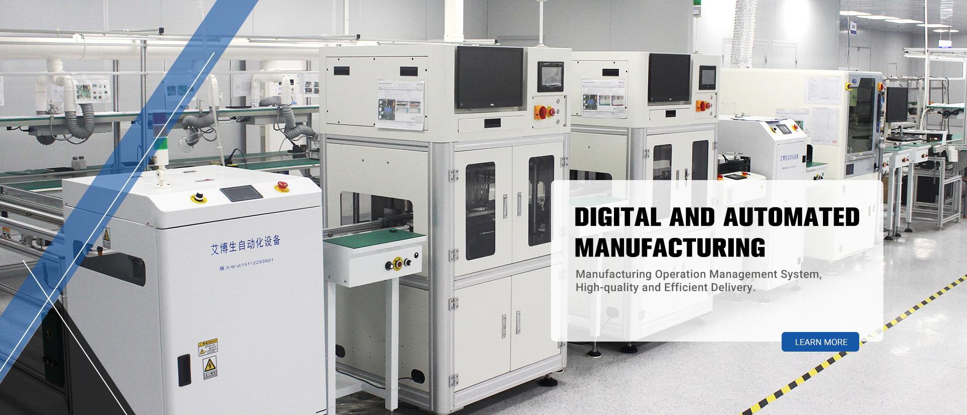
In the rapidly evolving world of electronics, surface mount technology (SMT) has become essential for modern device manufacturing. From initial concept to final delivery, the process involves meticulous planning and execution to ensure quality and efficiency. It begins with the design phase, where engineers utilize advanced software to create precise layouts, optimizing the arrangement of components on the printed circuit board (PCB). By employing simulation tools, potential issues can be addressed early, minimizing costly revisions later in the production line. Once the design is finalized, the fabrication stage commences. High-precision machinery is employed to produce PCBs with remarkable accuracy, ensuring that components, including resistors, capacitors, and ICs, are mounted securely. This is followed by the assembly process, where automated pick-and-place machines enhance speed and reliability, drastically reducing labor costs and production time. Quality control is paramount throughout this journey. Rigorous testing methods, including Automated Optical Inspection (AOI) and Functional Testing, are implemented to maintain high standards. Finally, efficient logistics and packaging ensure that products reach the global market promptly. With this comprehensive process, manufacturers can cater to diverse market demands, providing innovative, reliable, and high-performance electronic solutions for various applications across the globe.
Surface Mount PCB Application From Concept to Delivery
| Application Stage | Description | Key Considerations | Timeline |
|---|---|---|---|
| Concept Validation | Assessing the feasibility of the PCB design. | Market Research, Design Requirements | 1-2 Weeks |
| Design & Prototyping | Creating PCB layouts and initial prototypes. | Design Tools, Component Selection | 3-4 Weeks |
| Testing | Evaluating prototype performance under various conditions. | Testing Methods, Compliance Standards | 2-3 Weeks |
| Final Design Adjustments | Making necessary changes based on testing feedback. | Iterative Feedback, Design Reviews | 1-2 Weeks |
| Production | Manufacturing the final PCBs at scale. | Supply Chain Management, Quality Control | 4-6 Weeks |
| Delivery | Shipping the finished products to the client. | Logistics, Customer Handover | 1-2 Weeks |
Related Products
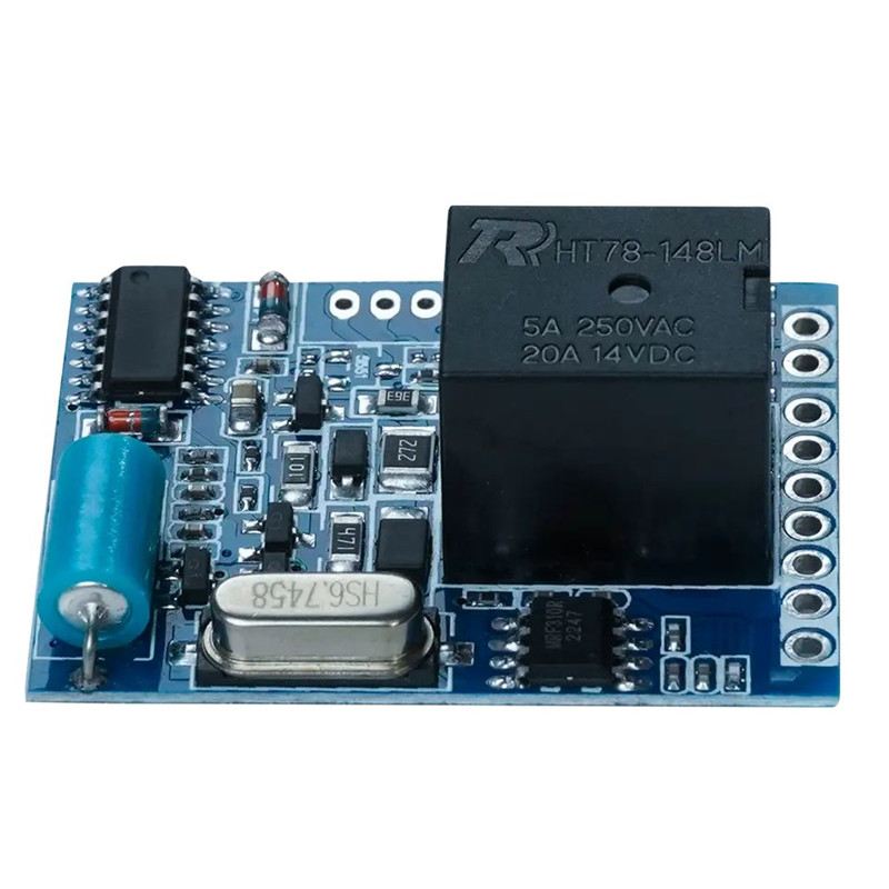
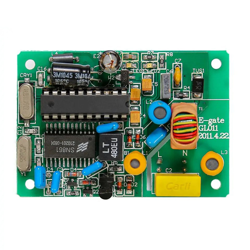

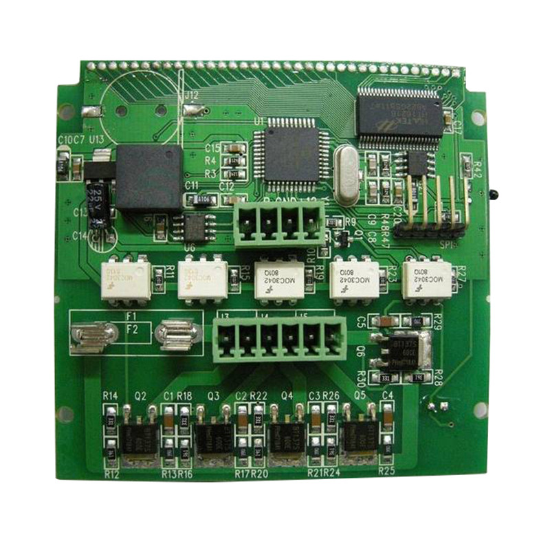
Surface Mount Pcb Industry Giant Winning in 2025
Top Selling Products
- Related Blog
- Reviews
- Reviews
