Efficient PCB Assembly Testing Methods for Factories: Enhancing Quality and Productivity
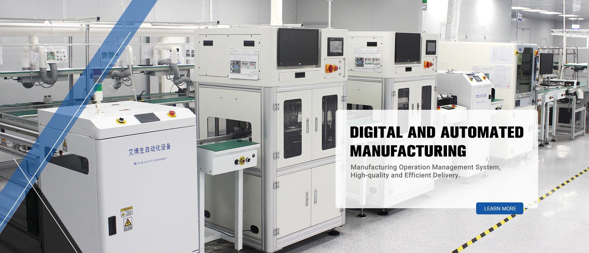
Introducing Zhuhai Xinrunda Electronics Co., Ltd., a prominent Chinese manufacturer, supplier, and factory specializing in PCB assembly testing methods. With years of expertise in the electronics industry, we pride ourselves on delivering high-quality products and exceptional customer service. At Zhuhai Xinrunda Electronics Co., Ltd., we understand the criticality of accurate testing methods in the PCB assembly process. Our state-of-the-art facility is equipped with advanced technology and operated by a team of skilled engineers and technicians. We offer a comprehensive range of testing methods, including functional testing, visual inspection, in-circuit testing, and more, to ensure the reliability and functionality of our PCB assemblies. As a trusted manufacturer and supplier, we adhere to stringent industry standards and guidelines, ensuring that our products meet the highest quality requirements. Our commitment to continuous improvement and innovation enables us to stay at the forefront of the evolving electronics market. Whether you require PCB assembly testing methods for consumer electronics, automotive applications, or industrial machinery, Zhuhai Xinrunda Electronics Co., Ltd. has the capabilities and resources to meet your specific needs. With our competitive pricing, efficient production processes, and reliable delivery, we strive to be your preferred partner in PCB assembly testing. Contact us today to learn more about our comprehensive range of PCB assembly testing methods and how we can fulfill your requirements.
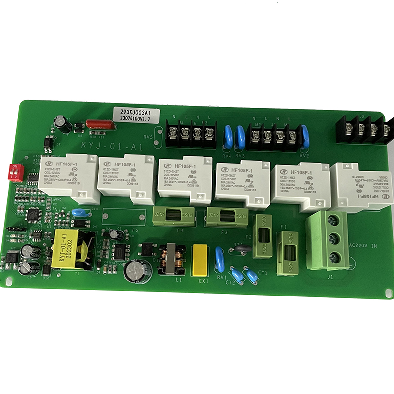
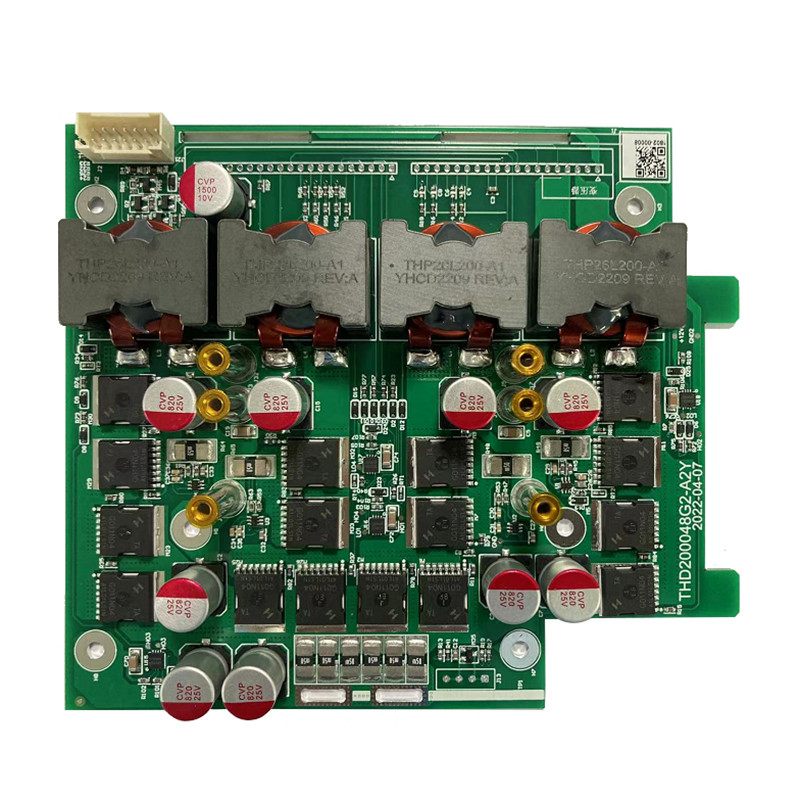
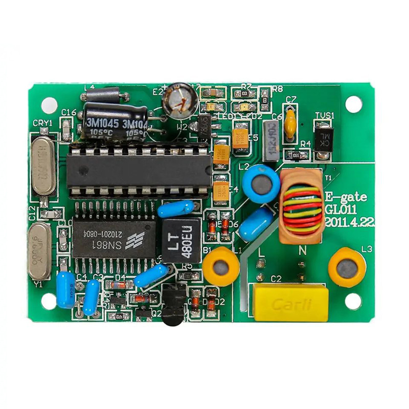
Related Products

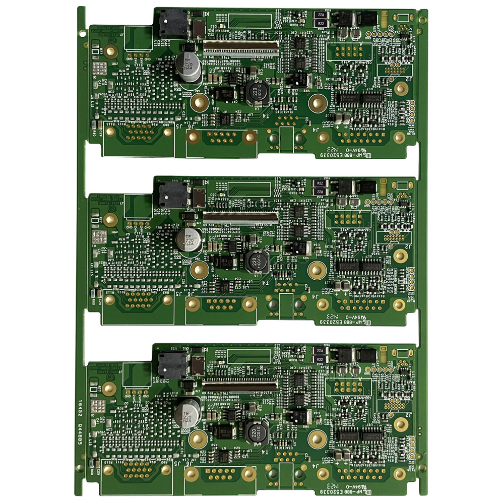
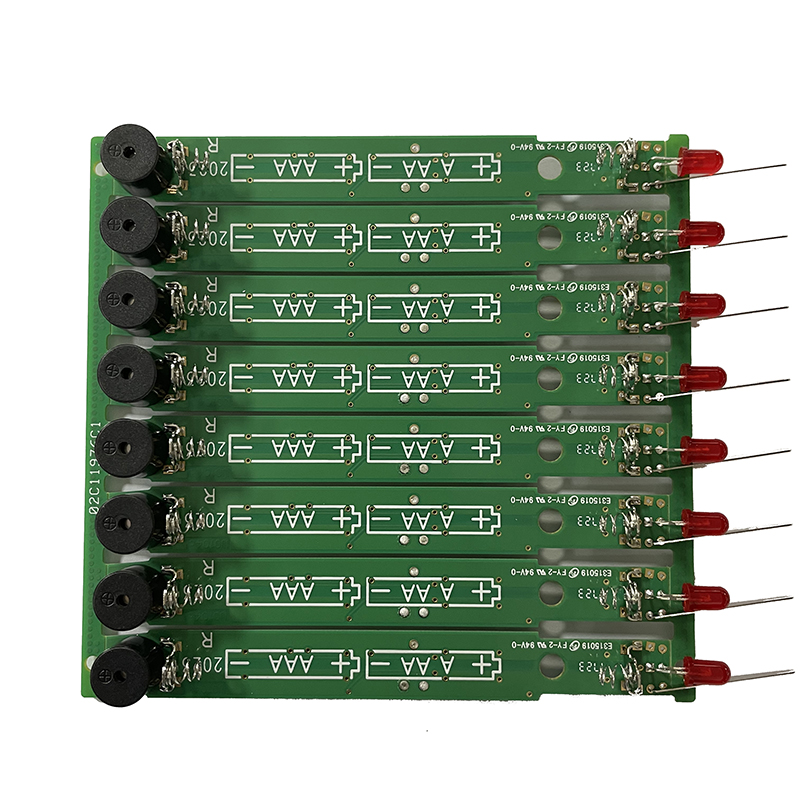


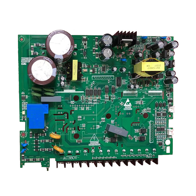
Top Selling Products

- Related Blog
- Reviews
