Pcb Assembly Steps Factory in China: Leading Manufacturer Guide
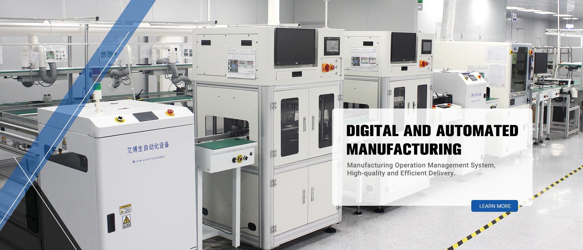
At our Pcb Assembly Steps Factory in China, we specialize in delivering high-quality manufacturing solutions tailored to your specific needs. I understand the importance of precision and efficiency in your projects. That's why we pride ourselves on our meticulous assembly process, ensuring every board meets strict quality standards. From prototyping to full-scale production, our team focuses on every step of the PCB assembly process. We utilize the latest technology and robust materials to provide reliable results. Working closely with you, we aim to streamline operations and lower costs without compromising on quality. Choosing us as your manufacturer means gaining a partner committed to excellence and customer satisfaction. Let’s take your project to the next level together – I’m excited to help bring your ideas to life with seamless assembly solutions tailored for your business.


Pcb Assembly Steps Factory Manufacturers You Can Rely On From Concept to Delivery
When it comes to PCB assembly, choosing a reliable manufacturer is crucial for ensuring that your projects move smoothly from concept to delivery. An efficient PCB assembly factory not only streamlines the process but also guarantees that your electronic products meet the necessary quality standards. A comprehensive approach to PCB manufacturing encompasses design support, prototyping, and final production, which helps bridge gaps often faced during development phases. Leading PCB assembly manufacturers leverage advanced technology and skilled personnel to optimize each step of the process. From initial design reviews to material selection and assembly techniques, these factories ensure that every detail is meticulously managed. This not only results in high-quality printed circuit boards but also enables faster turnaround times, critical for maintaining competitiveness in today’s rapid market cycles. Global procurement specialists can benefit from partnering with such PCB assembly manufacturers, as they offer a combination of technical expertise and robust supply chain management. By collaborating closely throughout the production stages, you can ensure that your ideas are transformed into functional devices that meet your specifications, ultimately contributing to a successful product launch in the global marketplace.
Pcb Assembly Steps Factory Manufacturers You Can Rely On From Concept to Delivery
| Step | Description | Key Tools/Equipment | Duration |
|---|---|---|---|
| 1 | Design PCB layout using CAD software. | CAD software, schematic capture | 1-2 weeks |
| 2 | Create a prototype PCB. | PCB fabrication equipment | 1 week |
| 3 | Assemble components onto the PCB. | Pick and place machine, soldering tools | 2-3 days |
| 4 | Test the assembled PCB for functionality. | Test equipment, automated test systems | 3-5 days |
| 5 | Enclose the PCB in its final casing. | Assembly tools, casing | 1 week |
| 6 | Prepare for final delivery. | Packaging materials | 2-3 days |
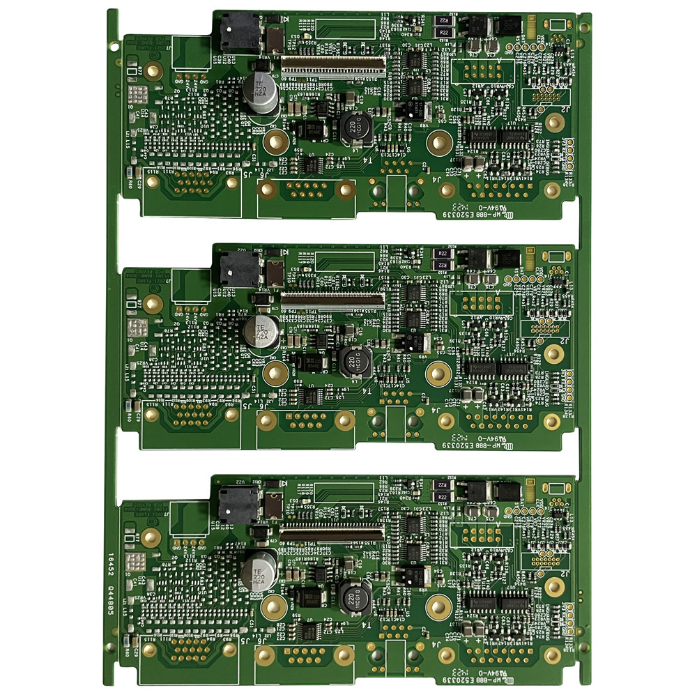
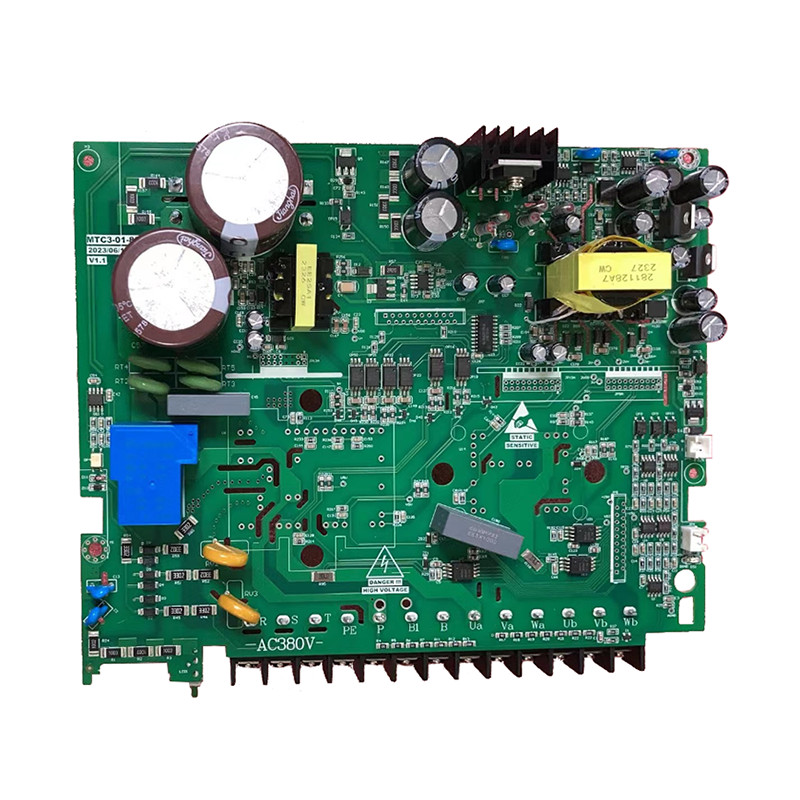
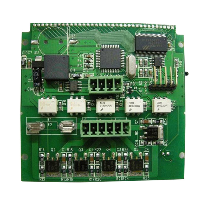
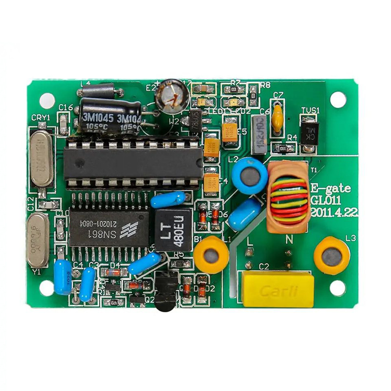
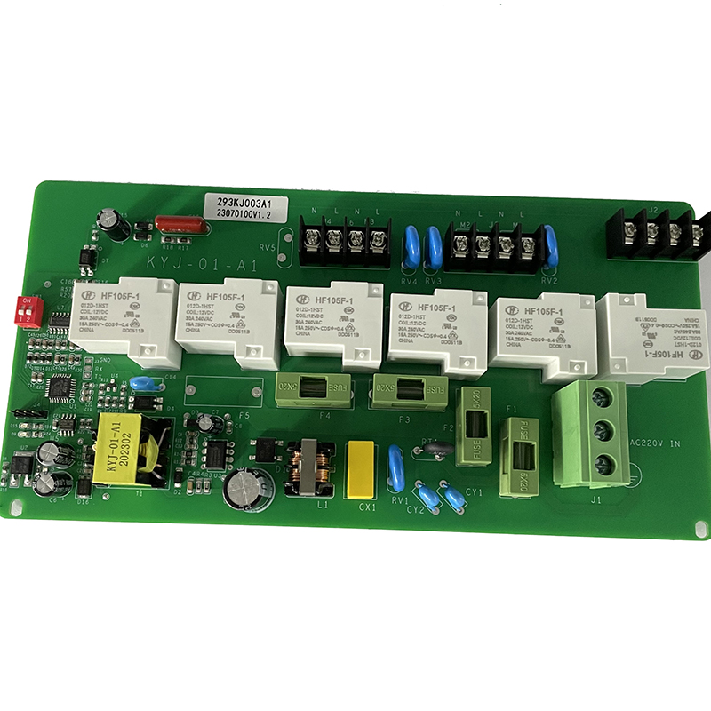
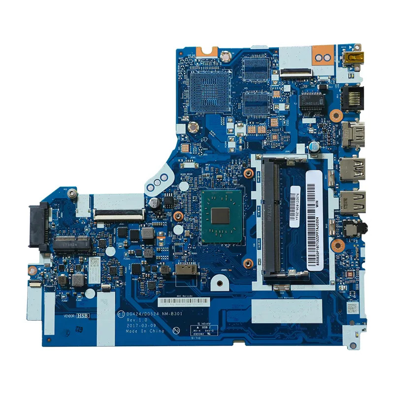
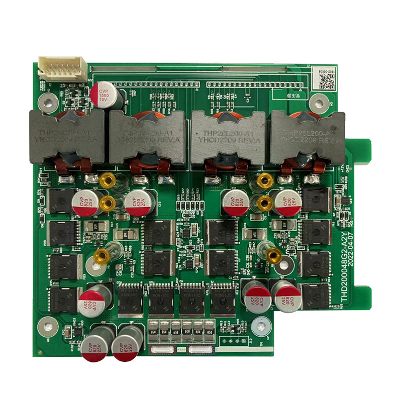
Related Products

Pcb Assembly Steps Factory For the Current Year Leads the Global Market
Top Selling Products
- Related Blog
- Reviews
- Reviews
