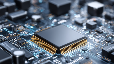
Designing and putting together printed circuit boards (or PCBs) with Pin Through Hole (PTH) tech is pretty important. This method basically makes sure that the electronic components stay connected solidly, which really boosts the circuit's reliability. But honestly, it’s not always a walk in the park—there can be quite a few challenges along the way.
Getting the hole sizes, spacing, and placement just right is a big deal. If they’re off even a little, it can cause connection issues later on. Soldering PTH parts also takes some finesse—bad solder joints? They’re usually the culprits behind failures. So paying close attention to every tiny detail during assembly is absolutely key.
A lot of companies tend to overlook these small but critical things. Sometimes they rush through the design phase without double-checking everything, which ends up costing them more in the long run due to revisions. Taking a moment to reflect on how things are done and what could be improved helps make better, more reliable designs. Honestly, every PTH PCB assembly is an opportunity to learn something new and maybe even come up with smarter ways to do it.
Pin through hole technology is crucial in PCB design. It establishes strong electrical connections between components. Understanding the specifics of this method can greatly enhance the functionality and reliability of your circuit boards. The hole diameter and plating quality play a significant role. If not done correctly, it may lead to weak joints or even failures.
Tip 1: Ensure hole sizes are precise. Overly large or small holes can disrupt component placement. This can be especially problematic during assembly. Avoid common mistakes in measurement when designing layouts.
Tip 2: Consider thermal and electrical performance. A well-implemented pin through hole can improve heat dissipation. However, improper spacing might lead to overheating and failures. Regular review of your design may help identify these issues early on.
Tip 3: Test your designs thoroughly. Prototypes can reveal unexpected flaws. Observing how components fit during assembly is vital. Sometimes, what looks good on paper doesn't translate well to the physical board. Remember, refining your design is just as important as the initial concept.
When designing a PCB, the size and plating of holes are critical. Choosing the right hole size affects component fit and assembly. A hole too small can cause misalignment during assembly. Conversely, an overly large hole may weaken the connection. A well-defined specification is essential.
Plating is another crucial aspect. Proper plating improves conductivity. It also prevents corrosion, enhancing the lifespan of the PCB. However, if the plating is too thick, it can lead to unexpected issues. Excess thickness may cause stress on the pad when components are soldered. Consideration of these factors is necessary for a successful design.
Mistakes are common in the design process. Skipping a thorough review of hole sizes can lead to assembly failures. Larger holes might require additional reinforcement. A balance must be struck. Without careful attention, even small errors can escalate into significant problems during assembly and performance testing. These nuances are not always obvious but deserve careful thought.
When designing printed circuit boards (PCBs), choosing the right pin types is crucial. The debate between through-hole and surface-mount technology (SMT) often surfaces. A 2021 IPC report stated that through-hole components are still used in about 30% of new designs. They provide robust connections and are easier to manipulate during assembly. However, they require more board space, which can be a limitation for compact designs.
Surface-mount technology offers smaller components that can fit into tighter spaces. According to a 2022 TechInsights analysis, 40% of PCB designs now favor SMT due to increased miniaturization and automation in manufacturing. Their compatibility with automated assembly makes them a popular choice. However, they can be challenging to work with in terms of soldering and require precise alignment.
Tip: Always assess the application requirements. If you need durability and easy accessibility, go for through-hole. For high-density layouts, surface-mount is the better option. Installing mixed technologies sometimes leads to a need for careful planning. Balancing space and performance can be tricky. Consider potential repairs; through-hole components are easier to replace if issues arise.
Proper hole placement on a PCB can significantly impact its performance and reliability. Critical components require optimal pin locations to ensure efficient current flow and thermal management. Misplaced holes can lead to signal integrity issues, especially in high-frequency applications. Designers should consider the connectivity paths. A longer trace can introduce unwanted resistance and inductance. Thus, keeping traces as short as possible is essential.
When designing, think about mechanical stress. Holes placed too close to edges may weaken the board structure. A poorly supported hole can lead to cracking under stress. Moreover, the material aspect matters. Different materials react differently to heat. This reaction can affect the hole’s integrity over time. It’s vital to strike a balance between several factors during the design process.
Lastly, testing and validation should not be overlooked. Even with careful planning, issues can arise. Prototype boards often reveal unseen problems. These findings are crucial for refining designs. Ignoring feedback from initial tests can result in costly mistakes later on. Adjustments after testing should be embraced, not feared. Each hole placement decision must be revisited and analyzed for overall improvement.
Thermal expansion is a critical aspect of PCB design. The materials used can expand or contract due to temperature changes. If hole integrity is compromised, it can lead to significant issues during assembly. When designing PCBs, consider the materials carefully. Different substances respond variably to heat. For instance, copper expands differently than fiberglass. This discrepancy can affect hole dimensions and cause stress.
As you design, it's essential to account for this expansion. One tip is to select materials with compatible thermal properties. Additionally, ensure clearances around holes are appropriate. Avoid tight tolerances that might lead to misalignment. Another suggestion is to use thermal simulation during the design phase. This practice can help you visualize how your PCB will react under varying conditions.
During assembly, monitor temperature changes. Rapid heating can impact hole integrity. Be cautious of soldering techniques that generate excessive heat. A slower, controlled approach may yield better results. Failure to consider these elements can lead to defects. A thorough understanding of thermal dynamics is vital.
Through-hole assembly remains an essential technique in PCB design. Effective soldering enhances reliability and performance. Various studies indicate that improper soldering techniques lead to over 30% of PCB failures. Each joint must be meticulously crafted. Adequate heat control is crucial. Too much heat can damage components, while too little leads to weak connections.
It's vital to ensure the right solder type and flux. Too much flux can create unwanted residues and affect performance. The ideal solder joint should be smooth and shiny. A dull appearance may suggest overheating. The solder should flow evenly around the joint. Visual inspection techniques reported by industry experts indicate that even small defects can significantly impact functionality.
Proper training for technicians is often overlooked. Many technicians may rush the process, leading to errors. An alarming 25% of technicians might not fully understand proper techniques. Regular training sessions can mitigate this issue. Use of precise temperature-controlled soldering irons is another best practice. These help maintain optimal temperatures, improving joint quality and reducing the chance of defects.
PCB design and assembly rely heavily on precise hole specifications. According to IPC standards, hole diameter tolerances can vary significantly based on manufacturing methods. For instance, the diameter tolerance for a plated through-hole can often range from ±0.05 mm to ±0.1 mm. This variance can impact the performance of electrical contacts and signal integrity. Proper understanding ensures compliance with industry standards, increasing reliability and efficiency.
Tips for effective PCB holes include validating hole sizes with prototypes. Mock testing helps identify whether designs meet functional requirements. Adjust designs based on iterative testing. Consider keeping specifications clear and concise. Documentation is key. Miscommunication can lead to costly errors.
The IPC-2221 standard emphasizes the importance of hole placement and layout. A common issue is hole misalignment, which can stem from inadequate design files. Reviewing design schematics before final submission can prevent such pitfalls. Focus on the critical nature of through-hole placement, especially in dense boards where space is limited. Ensuring adherence to these standards is crucial for the overall success of PCB projects.
| Dimension | Specification | Industry Standard | Common Material |
|---|---|---|---|
| Hole Diameter | 0.4mm to 3.0mm | IPC-4761 | FR-4 |
| Pad Size | 1.5mm to 6.0mm | IPC-6012 | Copper |
| Aspect Ratio | 1:6 to 1:10 | IPC-6012 | Epoxy |
| Plating Thickness | 1.5µm to 2.5µm | IPC-A-600 | Tin Lead |
The automotive industry is experiencing rapid advancements, particularly in the realm of electronic components, which are becoming increasingly integral to vehicle functionality and performance. Recent market trends highlight the growing demand for specialized PCB assembly services tailored for automotive applications. These components are crucial for enhancing features such as GPS navigation, audio systems, control mechanisms, and communication systems, which together contribute to a more connected and efficient driving experience.
High-quality PCB assembly services play a pivotal role in ensuring the reliability and performance of automotive electronics. Our offerings encompass a diverse range of applications, from GPS PCB assembly that enhances navigational precision to audio and video system assembly that elevates passenger entertainment. Additionally, our expertise in control system PCB assembly is essential for the seamless operation of various vehicle functions, while communication systems facilitate vital connectivity, ensuring both safety and convenience.
As the industry shifts towards more sophisticated electronic solutions, leveraging our PCB assembly services can provide manufacturers with the assurance of quality and reliability. This commitment to excellence empowers automotive producers to meet the evolving demands of consumers and stay ahead in a competitive market. With a focus on continuous improvement and innovation, we are poised to support the growth of automotive electronics in this dynamic environment.
: The product is designed to enhance daily activities. It aims at improving convenience for users.
The product operates through simple user interactions. Users engage with it to achieve desired outcomes.
Yes, the product may not work as expected in specific conditions. Users should test it in various settings.
Outdoor use is possible. However, performance might vary depending on weather conditions.
A limited warranty is provided. Users should review the terms carefully to understand the coverage.
Users can contact support for assistance. It's important to provide detailed descriptions of the problem.
No special skills are needed. Basic understanding of the instructions will suffice for most users.
Yes, many users report increased productivity. Results can vary based on individual usage patterns.
Cleaning is relatively straightforward. Regular maintenance ensures longevity but may require thoughtful effort.
Consider returning it, if possible. Reflect on how it fell short to make informed choices in the future.
The article "Pin Through Hole Tips for Effective PCB Design and Assembly" emphasizes the critical role of Pin Through Hole techniques in achieving efficient PCB design. It discusses key considerations such as hole size and plating, which are essential for ensuring reliable electrical connections during assembly. A thorough understanding of through-hole and surface-mount pin types helps designers make informed decisions based on their project requirements.
Moreover, the placement of holes significantly impacts PCB performance and reliability, necessitating careful planning to mitigate issues associated with thermal expansion that can affect hole integrity over time. The article also highlights best practices for soldering techniques in through-hole assembly and outlines industry standards that govern PCB hole specifications. By adhering to these guidelines, engineers can enhance the durability and functionality of their PCBs, leading to improved overall device performance.