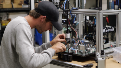
So, Pin Through Hole—often just called PTH—is basically a way to mount electronic components by sticking their metal leads through holes drilled in a PCB. Then you solder those leads to copper pads, usually on the opposite side. What you get is a solid, visible connection that you can actually inspect and, in most cases, fix with basic soldering tools. The name kind of says it all: the pins literally go through the board.
You’ll spot this approach in connectors, transformers, switches, and the bigger capacitors. The leads go right through the board and basically lock everything in place—that really helps if the assembly is going to deal with vibration or mechanical stress. Surface-mount technology, on the other hand, uses smaller pads and places components directly on the board, so it’s great for compact designs. But through-hole assembly is a different story: it needs drilled holes and eats up more board space. Honestly, it really depends—on the component, how it's made, and what you're using it for. There's no one-size-fits-all rule.
Say you're soldering a resistor lead—you push it through the hole, trim the excess, and make the joint. A good joint should look shiny, but if it's dull or cracked, that's a red flag. Still, looks can be deceiving; appearance only gets you so far. You can't just eyeball it and call it reliable. You still need proper inspection, decent materials, and solid technique. Honestly, the process is simple enough to grasp, but that doesn't mean it's easier or better once you're doing it on a large scale. When you're picking a material, it's not just about the specs. You've gotta weigh strength, how easy it is to repair, the board layout, and the manufacturing cost. Honestly, the right call can be way less obvious than just comparing numbers on a page.
Pin-through-hole (PTH) technology mounts components by inserting their metal leads through drilled holes in a printed circuit board. Copper plating inside each hole connects the lead to conductive layers, while solder forms an electrical and mechanical joint on the board’s opposite side. Some holes connect several layers; others connect only specific copper paths.
The core principle is direct physical contact: a lead passes through the board, and solder secures it to a surrounding pad. This creates sturdy joints, useful for connectors, transformers, and parts exposed to vibration or repeated handling. The trade-off is real. Drilling and soldering take space and can add assembly time compared with surface mounting. Grand View Research’s 2024 Printed Circuit Board market report valued the global PCB market at about $73.3 billion in 2023. That figure describes the wider market, not PTH adoption, so it should not be read as evidence of how often this method is used.
Tips: Check the hole diameter against the component lead and plating tolerance. A lead that fits too tightly can damage the plated barrel during assembly. PTH is robust, but not automatically better; I would review access, board space, and repair needs before choosing it.
What Is Pin Through Hole Technology?
Key Components of a Through-Hole Connection
A through-hole connection joins a component lead to conductive copper on a printed circuit board. The lead passes through a drilled opening, then solder bonds it to a pad. In a plated-through hole, a thin copper barrel lines the opening and connects copper layers. The lead, barrel, pad, and solder fillet work together. Each has a job.
Tips: Use enough solder to form a smooth, gently concave fillet around the lead. Check that solder wets both the lead and pad. A dull surface alone does not prove a bad joint, but gaps or exposed lead sections deserve a closer look.
Hole size matters. Too little clearance makes insertion difficult; too much can weaken the mechanical fit. Heat also travels through the lead and copper barrel, so a small pad may need careful, even heating. A tidy joint can still hide poor wetting underneath. That part is easy to miss, and visual inspection has limits. For critical assemblies, electrical continuity checks and suitable inspection methods add confidence.
In pin-through-hole assembly, each component lead is guided into a drilled opening in the circuit board. The holes may have copper-plated walls, called barrels, which connect board layers electrically. A technician checks the component’s orientation and seats it evenly. Small details matter. A bent lead or misplaced part can slow the line and strain the board.
Soldering creates the mechanical and electrical connection. In wave soldering, the board’s underside passes over a controlled wave of molten solder. For smaller runs or selected joints, an operator may heat the pad and lead with an iron, then feed in solder. Flux helps clean the metal surfaces so solder can wet them properly. It should flow around the lead and form a visible fillet, not sit as a loose bead. Too much heat can damage pads; too little can leave a weak joint.
After soldering, assemblers inspect joints for gaps, dull surfaces, bridges, and uneven fillets. Magnification helps, but appearance alone cannot confirm every connection inside a plated barrel. That limitation is easy to overlook. Process settings, clean materials, and consistent inspection all matter, yet no single visual check catches everything. When a board is critical, electrical testing can reveal faults that the eye misses.
Common Through-Hole Component and Pin Types
Through-hole components pass metal leads through drilled circuit-board holes, where solder secures them on the opposite side. Common examples include axial resistors, radial capacitors, diodes, transformers, relays, and dual-in-line integrated circuits. Axial parts have leads extending from both ends; radial parts have leads grouped on one side. That small difference affects board layout and how a component sits among nearby parts.
Pins vary too. Straight pins suit vertical mounting, while right-angle pins turn toward a board edge or another connection. Round pins fit many sockets; square pins can provide a firmer contact, though insertion force matters. Connector pins may be solder-tail or press-fit types, and press-fit pins rely on mechanical interference rather than solder. IPC workmanship guidance emphasizes inspecting soldered connections, not just checking whether a lead passes through a hole. A neat-looking joint can still be weak.
Through-hole choices remain relevant as electronic production grows. The WSTS Fall 2024 semiconductor market forecast projected global sales of about $626 billion for 2024. That figure does not measure through-hole use, but it reflects the scale of electronics manufacturing where component selection matters. For repairable equipment or parts exposed to vibration, a sturdy lead can help. Yet thicker pins take more board space. Easy to overlook. Check the hole diameter, pad size, and assembly method together; the pin that seems strongest may not be the best fit.
Through-hole components have leads that pass through holes in a circuit board and are soldered on the opposite side. This chart compares typical adjacent lead pitches for several common component types. Actual dimensions can vary by package; check the component datasheet before designing a PCB.
Through-hole assembly creates a direct mechanical connection: component leads pass through drilled board holes and are soldered on the opposite side. This can suit connectors, switches, and parts exposed to vibration or repeated handling. The joint is also accessible for visual inspection and repair. Strong, visible connections.
IPC-A-610H, the industry’s Acceptability of Electronic Assemblies standard, uses 75% vertical solder fill as an acceptance criterion for applicable plated-through-hole joints. That figure gives inspectors a measurable check, but it is not a guarantee of long-term reliability. Board thickness, hole size, lead fit, and soldering conditions still matter.
The trade-off is space and production speed. Drilled holes occupy board area, and inserting many leads can slow assembly compared with surface mounting. Large components may also draw heat away during soldering, making consistent joints harder to achieve. That can mean extra process control. Through-hole is not automatically the stronger choice; a poorly filled barrel or stressed lead can still fail. Designers should match the method to the component’s mechanical load, board density, and repair needs. One detail is easy to overlook: every added hole constrains routing on multiple board layers.
| Dimension | Through-Hole Assembly | Benefits | Limitations and Considerations |
|---|---|---|---|
| How it works | Component leads or pins pass through drilled holes in a printed circuit board (PCB) and are soldered to conductive pads, usually on the opposite side. | The lead passes through the board, creating a direct mechanical connection as well as an electrical one. | Each lead requires a corresponding drilled hole, which affects board layout and fabrication. |
| Mechanical strength | Leads are anchored through the PCB rather than resting only on surface pads. | Often a good choice for parts subject to insertion, pulling, vibration, or other mechanical stress, such as connectors and switches. | Mechanical strength still depends on the component, solder joint, PCB construction, and expected loads; through-hole mounting is not a guarantee against failure. |
| Board space and density | Holes and component leads occupy board area and may require clearance on both sides. | Can be practical for larger components whose size already sets the required layout area. | Typically allows lower component density than surface-mount assembly and can restrict routing space, especially on compact boards. |
| Assembly methods | Components may be inserted by hand or machine, then soldered by hand, wave soldering, or selective soldering. | Suitable for prototypes and for production processes that need to accommodate through-hole parts. | Insertion and soldering can add process steps. In high-volume production, through-hole assembly may take more time than surface-mount assembly, depending on the design and equipment. |
| Inspection and rework | Leads and solder joints are often accessible for visual inspection and repair. | Individual components can be straightforward to replace when the board layout provides access. | Removing a part can require clearing solder from its holes. Rework may be difficult on densely populated or multilayer boards and can damage pads if performed improperly. |
| Electrical and thermal performance | Lead size, material, hole plating, and solder-joint design determine the electrical and thermal path. | Some through-hole components offer robust leads and are available in forms suited to higher current or power applications. | Performance is not inherent to the mounting method alone. Current capacity, heat dissipation, and reliability must be verified for the specific component and PCB design. |
| Typical applications | Commonly used for connectors, transformers, power components, and parts that benefit from strong mechanical anchoring. | Useful when component size, mechanical loading, or assembly requirements favor leads that pass through the PCB. | May be less suitable as the primary mounting method for compact, densely populated electronics; mixed through-hole and surface-mount designs are also common. |
Pin through-hole technology remains useful where components must withstand physical stress. Component leads pass through drilled board holes and are soldered to conductive pads. This creates a firm connection for heavy parts, including transformers, relays, and power components. It also suits board-edge connectors, where repeated plugging can strain solder joints. That matters.
Grand View Research estimated the global printed circuit board market at USD 76.2 billion in 2023, with a projected 5.3% compound annual growth rate from 2024 to 2030. This broad market figure does not measure through-hole use specifically. Still, it shows the scale of the electronics sector in which designers balance durability, cost, and assembly needs.
In industrial control equipment, through-hole terminals can make field wiring easier to secure and inspect. Repair technicians may also find larger joints easier to rework than tiny surface-mounted parts.
A caveat remains: drilled holes consume board space, and manual assembly can raise labor time. IPC-A-610 provides workmanship criteria for soldered electronic assemblies, but designers must still evaluate each device’s loads, vibration, and production process.
The trade-off is easy to underestimate.
Each lead passes through a drilled hole and is soldered to a pad on the other side. The lead should sit evenly.
Flux cleans metal surfaces so solder can spread around the lead. A smooth fillet is the goal, not a loose bead.
They look for gaps, dull surfaces, solder bridges, and uneven fillets. Magnification helps. Looks can still mislead.
No. A joint may look fine while a hidden connection inside the plated hole remains faulty. Electrical testing can catch issues the eye misses.
Leads pass through the board, creating a direct mechanical connection. This can suit transformers, switches, and board-edge connectors. Repeated stress still matters.
Drilled holes take up board space and restrict routing across layers. Inserting many leads can also slow production. It is easy to underestimate that cost.
No. A 75% vertical solder-fill criterion applies to certain plated-through-hole joints, but it does not guarantee long-term reliability. Fit, board thickness, and heat also matter.
Larger leads and visible joints can be easier to inspect and rework. Still, a stressed lead or poorly filled hole can fail. No method is foolproof.
Pin Through Hole technology is a method of mounting electronic components by inserting their metal pins through holes in a circuit board and soldering them to conductive pads. A reliable connection depends on the component leads, plated or unplated board holes, copper pads, and solder joints working together. During assembly, pins are aligned with the holes, inserted to the correct depth, and soldered—by hand or with a production process—so they remain secure and electrically connected.
Common through-hole parts include resistors, capacitors, connectors, and integrated circuits, with leads such as straight, bent, or shaped pins. This assembly method offers strong mechanical support, straightforward inspection, and convenient repair, making it useful for parts that face physical stress. Its limitations include larger board space, holes that can restrict routing, and assembly that may take more time than surface mounting. Through-hole components are often found in power equipment, prototypes, educational projects, and devices where durability or easy servicing is important.