Welcome to our website.
0%

When it comes to electronics, the Double In-Line Package (or DIP, for short) is still a pretty popular option for lots of different projects. I remember Robert Jones—who's a real expert over at Tech Innovations Inc.—once mentioned, “DIPs are straightforward and reliable, which makes them super handy for all kinds of designs.” Honestly, that’s pretty spot on for engineers looking for simple, effective solutions.

Now, DIPs do come with their fair share of perks. They're generally easy to handle and slot right into circuit boards without much fuss. But, and here’s the catch, they’re not always the best fit for every project. With modern designs leaning towards smaller, more compact devices, the size of DIPs can be a bit of a drawback. So, engineers really need to consider these factors carefully before deciding.

All in all, getting a good grasp of what the Double In-Line Package has to offer—its strengths and its limitations—is super important. Knowing when and where to use it can make a real difference. Sometimes, taking a moment to think things through can lead to better, more efficient designs down the road.

Double In-Line Package Tips for Effective Use and Benefits?

Understanding Double In-Line Package (DIP) Basics

Double In-Line Package Tips for Effective Use and Benefits?

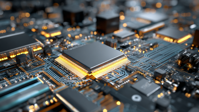
The Double In-Line Package (DIP) is a versatile component commonly used in electronics. Its rectangular shape allows it to be easily integrated into circuit boards. A recent industry report indicates that the DIP market is expected to grow at a compound annual growth rate of 5% over the next five years. This growth is fueled by the rising demand for compact electronic devices.

DIPs come with several advantages. They provide sturdy connections and ease of soldering, making them suitable for prototyping. Legs on both sides facilitate easy handling. However, a downside is their space consumption. As boards become more crowded, the DIP might struggle to fit. Additionally, the thermal performance can be less effective compared to newer package types.

Understanding the DIP's basics is essential. Each DIP varies in pin count and dimensions. Thorough knowledge of specifications is vital for effective usage. Some engineers may overlook these details, leading to errors in design. Practical application often reveals gaps in understanding, encouraging further learning and adaptation. It's crucial to assess the practical benefits while remaining aware of its limitations.

Key Benefits of Using Double In-Line Packages

Double In-Line Packages (DIPs) provide various advantages in electronics design. They are compact and easy to handle, making them ideal for circuit boards with space constraints. The two rows of pins help save valuable board space. This design facilitates efficient routing of traces, which enhances signal integrity.

One key benefit of DIPs is their versatility. They can house different components, from simple resistors to complex microcontrollers. Manufacturers often prefer them for prototyping due to their easy soldering process. Additionally, DIPs support manual assembly without specialized tools, which can be a double-edged sword. The human touch can lead to errors. Assembly mistakes can complicate the debugging process.

Another essential aspect of DIPs is their accessibility. They are widely available and often cost-effective. However, with the rise of surface-mount technology, some might question their relevance. DIPs can occupy more space, impacting designs aiming for miniaturization. Yet, for hobbyists and educational purposes, they remain invaluable. Understanding their role in modern electronics is crucial, even as trends evolve.

Common Applications of DIP in Electronics

Double In-Line Packages (DIPs) are widely used in electronics. They house integrated circuits in a dual-row configuration. This design facilitates easy installation and soldering on printed circuit boards. Commonly, you'll find DIPs in older computer systems, consumer electronics, and various DIY projects. Their versatility makes them a favorite among hobbyists and engineers alike.

When working with DIPs, consider a few tips for effective use. Ensure your PCB design accommodates the pin spacing. A mismatch can lead to misalignment, making soldering difficult. Additionally, use the right soldering technique. Too much heat can damage the components. Always verify the component orientation before soldering, as incorrect placement can cause malfunctions.

DIPs also find applications in educational tools and prototyping. They allow students to learn about circuits hands-on. In prototyping, DIPs provide an efficient way to test concepts. However, fitting them into compact spaces can be challenging. Always plan for the size and layout, keeping accessibility in mind. Adapting to these considerations helps maximize the benefits of DIPs.

Common Applications of DIP in Electronics

Tips for Selecting the Right DIP for Your Project

When selecting the right Double In-Line Package (DIP) for your project, consider the specific needs of your design. The size and layout of your PCB play a critical role. Measure the available space carefully. Check the pin count of your chosen DIP. It should match your project requirements. Sometimes, a DIP may have more pins than necessary. This could lead to wasted space.

Additionally, think about the intended application of your device. A DIP suitable for a hobby project may not be ideal for industrial use. Evaluate factors like temperature and voltage ratings. Some DIPs may be less reliable than others in harsh conditions. It’s important to ensure your chosen DIP can handle the stress of your application.

Look into the manufacturing process of the DIP too. Different methods yield different levels of quality and consistency. Researching options can save you hassle later on. Ensure to verify your selections before finalizing. A small oversight can lead to significant issues. Always have a backup plan. Consider prototypes to test designs before full-scale production.

Best Practices for Handling and Soldering DIPs

Handling and soldering double in-line packages (DIPs) require precision and care. Start by ensuring a clean workspace. Dust and debris can lead to poor connections. Use a soft cloth to wipe the area. Good lighting is also crucial. It prevents mistakes when placing components.

When soldering, be mindful of the heat. Too much can damage the DIP. A soldering iron tip temperature around 350 degrees Celsius works well. Apply heat for just a second or two. This minimizes the risk of overheating.

Practice is vital. Beginners often struggle with melting solder. Keep the soldering wire close to the joint. Too far away can lead to cold solder joints. These joints appear dull and can fail easily. Check each connection thoroughly. A microscope helps identify any faults. Inspecting ensures reliable circuits in the end product.

Common Challenges and Solutions in DIP Usage

Double In-Line Packages (DIPs) are widely used in electronics due to their simplicity. However, the effective use of DIPs brings its own set of challenges. One common issue is pin misalignment during manufacturing. According to industry reports, misalignment can lead to up to 10% failure rates in PCB assemblies. This highlights the need for precise placement in production.

Another challenge is thermal management. DIPs can generate significant heat, which may lead to performance degradation. It’s vital to ensure that boards incorporate adequate cooling solutions. Reports suggest that incorporating heat sinks can reduce thermal issues by as much as 30%. Ultimately, attention to thermal design is crucial.

Here are some tips for optimizing DIP usage:

  • Ensure measurements are precise when designing the PCB layout.
  • Regularly inspect solder joints to prevent conductivity issues.
  • Implement a testing phase post-assembly to identify and rectify defects early.

While DIPs offer many benefits, awareness of these challenges is essential. Needing to refine manufacturing processes can lead to improved reliability. Overcoming these obstacles is part of ensuring DIPs remain effective in diverse applications.

Future Trends in Double In-Line Package Technology

Double In-Line Package Tips for Effective Use and Benefits?

The future of Double In-Line Package (DIP) technology looks promising, yet it poses some challenges. As electronics become smaller, the need for compact and efficient packaging increases. DIP is adapting to these demands, but engineers must rethink design strategies. While traditional DIP offers advantages in stability and ease of handling, the rise of surface-mounted devices is hard to ignore. This shift forces DIP to stay relevant.

Moreover, sustainability is becoming a core concern. Many manufacturers are exploring eco-friendly materials for packaging. This change could impact performance and longevity. Engineers must balance environmental responsibility with the technical requirements of modern applications. There's room for innovation as designers develop new features that can meet both demands. However, using new materials may require additional testing and validation.

Collaboration is key in this evolving landscape. Engineers, manufacturers, and designers need to communicate effectively. Rapid prototyping can facilitate feedback loops, allowing for quicker adjustments. It's important to learn from past designs and openly discuss failures. This reflective practice can lead to more informed decisions, enhancing the overall effectiveness of DIP technology. Embracing these future trends will shape the next generation of electronic devices with a focus on efficiency and sustainability.

FAQS

: What is the main purpose of this product?

: This product aims to improve daily efficiency. It simplifies tasks and saves time.

How can I use this product effectively?

Start with the user guide. Familiarize yourself with its features and functions.

Are there any specific maintenance tips?

Yes, regular cleaning is essential. Ensure all parts are in working order frequently.

What should I do if I encounter an issue?

Refer to the troubleshooting section. Often, issues can be resolved easily with basic steps.

Is there a customer support option available?

Yes, support is available via email or live chat. They respond within a reasonable timeframe.

How often should I replace components?

Component lifespan varies. Monitor performance for signs of wear and replace as needed.

Conclusion

The article "Double In-Line Package Tips for Effective Use and Benefits" provides a comprehensive overview of the Double In-Line Package (DIP), detailing its fundamental characteristics and advantages in electronic applications. DIPs are favored for their ease of use in prototyping and their robust design, making them suitable for a wide range of electronic devices.

The article discusses common applications of DIPs, offering insights on how to choose the right package for specific projects and highlighting best practices for handling and soldering these components. Additionally, it addresses common challenges faced during DIP usage and presents potential solutions to overcome these obstacles. With a glance at future trends in DIP technology, the article emphasizes the ongoing relevance and adaptability of Double In-Line Packages in the evolving landscape of electronics.

Ethan

Ethan

Ethan is a dedicated marketing professional with a deep expertise in the electronics manufacturing sector at Zhuhai Xinrunda Electronics, a high-tech company established in 2004. With a strong commitment to providing top-notch electronic manufacturing services, including Surface Mount Technology......
Previous Mastering Import Export Certification for Best Small Batch Pcb Assembly Solutions