The Double In-Line Package (DIP) is honestly a pretty important part of electronics manufacturing. It acts like a bridge between the good old traditional methods and the newer, more advanced tech. I mean, with the global market for electronic manufacturing services expected to hit a whopping $2 trillion by 2026, finding efficient and reliable ways to package components has become more crucial than ever. Anyway, Zhuhai Xinrunda Electronics Co., Ltd., which was founded back in 2004, is really leading the charge in this area. They offer all sorts of manufacturing services—like SMT, PTH, and COB—that help bring these devices to life. Using DIP makes it way easier to slot integrated circuits into various printed circuit boards, and it also makes scaling up production a lot smoother. As everything in this industry keeps shrinking—devices getting smaller but more feature-packed—it’s super important for manufacturers to really get what the Double In-Line Package means. Otherwise, staying competitive in such a fast-changing market is going to be a real challenge.

Understanding Double In-Line Package (DIP) Design and Structure
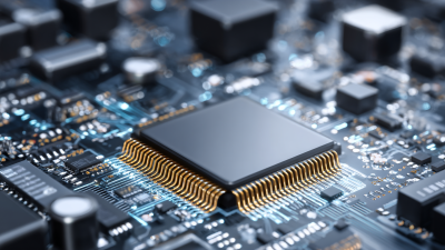
The Double In-Line Package, or DIP for short, is one of those classic electronic components everyone’s seen—it's everywhere! Basically, it’s a rectangular piece with two rows of pins running parallel, which makes it pretty straightforward to handle and solder onto a circuit board. I read in a recent market report from ResearchAndMarkets that the global DIP market is expected to grow at around 4.5% annually from 2022 all the way through 2030. This makes sense because, even after all these years, DIP still pops up in a bunch of areas like consumer electronics, car gadgets, and industrial gear.
What’s cool about DIP is its design—not only does it make heat dissipation simpler, but it also keeps electrical performance pretty reliable, which is a big deal for modern devices. The pins usually sit about 2.54 mm apart, so they play nicely with most PCB layouts out there. Plus, thanks to the new manufacturing methods, these components have become even more dependable, which is probably why they’re still so popular. In fact, a 2023 survey shows that nearly 60% of electronics makers prefer using DIP for prototyping because it’s just easier to work with and doesn’t break the bank. All in all, it’s safe to say that DIP still holds a pretty important place in the ongoing evolution of electronics manufacturing.


Exploring the Benefits and Process of Automated Products PCB Assembly Service in Modern Manufacturing
In modern manufacturing, the integration of automated products into the PCB assembly process offers numerous advantages, particularly when it comes to efficiency, quality, and adaptability. Automated PCB assembly services, like those provided by XINRUNDA, leverage advanced technologies that streamline production workflows and minimize the risk of human error. A report from Grand View Research indicates that the global PCB market is expected to reach $85.8 billion by 2027, driven by the demand for electronic devices and automation. This underscores the importance of reliable PCB assembly solutions that can keep pace with evolving market needs.
A vital component of developing effective industrial PCB assemblies is the collaboration between designers and contract manufacturers (CMs). At XINRUNDA, our turnkey prototyping service emphasizes a close partnership, enabling designers to take the lead in the manufacturing process. This collaborative approach allows for rapid adjustments to design specifications, ensuring that changes can be implemented quickly and seamlessly, thereby reducing time-to-market. As an illustration, our high-quality manufacturing capabilities encompass the production of PCBs for hard, soft, or integrated automation systems, tailored to meet diverse application requirements.
Furthermore, industry reports from IPC reveal that automated assembly processes can enhance production speed by up to 30% compared to traditional methods, while also improving accuracy and consistency in assembly. This is particularly critical in sectors such as automotive and consumer electronics, where precision and reliability are paramount. By embracing automated PCB assembly services, manufacturers can not only achieve higher production standards but also gain a competitive edge in the fast-paced manufacturing landscape.

FAQS
: The primary benefits of using DIP include ease of integration into circuit boards, excellent heat dissipation, versatility in applications, durability, and a robust connection ideal for products exposed to harsh environments.
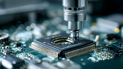
DIP streamlines manufacturing by enabling automated machinery to insert components into PCBs efficiently, utilizing wave soldering techniques to solidify connections quickly, thus improving reliability and reducing human error.
DIP is commonly used in a wide range of applications, including industrial machinery, consumer electronics, and innovative areas like smart electronic textiles (e-textiles) for health monitoring.
DIP allows for seamless integration of electronic functions into fabrics, providing improved electrical connectivity and compact design, which enhances user experience in wearable technology.
DIP switches are increasingly utilized in various devices for their customizability and ease of modification, making them suitable for both retro-inspired gadgets and advanced monitoring systems.
Designers should focus on user interface and interaction, ensuring that the technology is accessible and easy to operate for a broader audience.
The larger physical size of the DIP allows for better heat dissipation, which is crucial for the reliability and longevity of complex electronic circuits.
Automated machinery enhances the speed and accuracy of placing DIPs into pre-drilled holes on PCBs, leading to increased production efficiency and reduced errors during assembly.
DIP can coexist with SMT on the same circuit board, allowing for a hybrid design approach that maximizes design flexibility and minimizes production costs.
The robust connection provided by DIP makes it ideal for products that require frequent handling or are exposed to harsh conditions, ensuring dependable performance.
Conclusion
The Double In-Line Package, or DIP for short, is one of those electronic component packages that’s been around for ages and really changed the way electronics are made. Its straightforward design makes it super easy to plug onto printed circuit boards, so it’s no wonder it’s such a popular choice across different applications. Some of the biggest perks? Well, they include its reliability, affordability, and how well it plays with both automated machines and good old manual assembly. When you compare DIP to other packaging options out there, it really shines because of its simple, rugged design—kind of like the dependable old-timer in the industry.
As manufacturing tech keeps marching forward, people are finding more innovative ways to use DIP in modern gadgets and devices. This means better functionality and performance, whether it’s in everyday consumer electronics or heavy-duty industrial gear. Companies like Zhuhai Xinrunda Electronics Co., Ltd., which started back in 2004, are really leading the charge here. They offer a whole range of electronics manufacturing services, including those tailored specifically for DIP components. Looking ahead, it’s pretty clear that DIP isn’t going anywhere anytime soon. It’ll keep evolving and finding new spots in the high-tech manufacturing scene, becoming ever more integrated into how we build the electronics of tomorrow.
Related Posts
-

Maximizing Value: How the Best Double In Line Package Reduces Repair Costs with Superior After-Sales Service
-
7 Essential Tips for Choosing the Right Electronic Assembly Services
-

Exploring PCBA Assembly Trends at the 138th Canton Fair 2025: Insights for Industry Growth
-

Exploring Industry Standards: Digital Insights into the Top Reasons for Choosing China’s One-Stop PCB Assembly Service
-

Challenges of Sourcing the Best PCB Design and Assembly for Your Business Needs
-
Top Strategies for Optimizing Your Electromechanical Assembly Service Efficiency
