Welcome to our website.
0%

The Double In-Line Package (DIP) is honestly one of those classic packaging styles that’s been a go-to in electronics for ages. It’s pretty recognizable—with its two straight rows of pins—making it easy to handle and solder, which is probably why lots of folks prefer it for all sorts of projects. If you think back to the early days of integrated circuits, the DIP was pretty much the standard, and even now, it still pops up, especially when you're messing around in school labs or sketching out prototypes. Its simple design makes it super straightforward to fit onto printed circuit boards, so it’s still hanging around in the tech scene.

One big perk of the DIP is that it can hold quite a few pins—perfect for connecting all those different parts of a circuit efficiently. Not only does this mean you can pack in more connections, but it also helps keep things running smoothly by reducing signal noise and boosting reliability. Plus, since it's designed with through-hole mounting, it’s quite sturdy, making devices more durable and reliable over time, even in tougher environments. As electronic devices become more complex and demand better performance, getting to know the ins and outs of the Double In-Line Package is pretty important for engineers and manufacturers who want to stay ahead of the game.

What is a Double In-Line Package and Its Advantages in Electronics

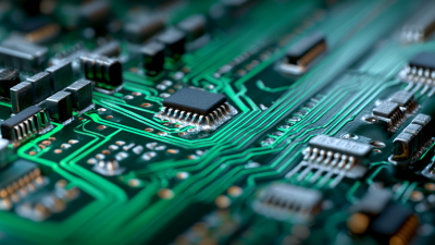
Definition and Structure of Double In-Line Package (DIP)

What is a Double In-Line Package and Its Advantages in Electronics

A Double In-Line Package (DIP) is a type of electronic component packaging that features two parallel rows of connecting pins. The standard widths of DIP packages are typically 0.6 inches (15.24 mm) or 0.3 inches (7.62 mm), accommodating various pin counts, commonly ranging from 8 to 40 pins. The design provides an effective means for mounting integrated circuits (ICs) onto printed circuit boards (PCBs), allowing for both through-hole and surface-mount configurations. According to a report from the International Electrochemical Commission, the adoption of DIP for both low to medium production volumes remains prevalent due to its simplicity and robustness in circuit design.

The structure of a DIP facilitates enhanced thermal management and electrical performance, as it typically possesses a flat, rectangular shape that allows for better heat dissipation compared to other packages. The lead spacing of DIPs, often standardized at 2.54 mm (0.1 inches), enables easy alignment and soldering during assembly. Furthermore, the accessibility of the pins makes it straightforward for testing and prototyping, aligning with data from the Institute of Electrical and Electronics Engineers, which suggests that well-optimized DIP structures can reduce assembly time by up to 30%. Its prevalence in educational settings and prototype development is attributed to these advantages, making it a favored choice for engineers and developers working on innovative electronic solutions.

Historical Development of Double In-Line Package Technology

The Double In-Line Package (DIP) technology has its roots in the rapidly evolving landscape of electronics in the mid-20th century. Introduced in the 1960s, the DIP was a response to the need for more compact and efficient packaging of integrated circuits. Researchers and engineers sought a solution that would not only minimize space but also enhance the ease of manufacturing and assembly. The design allowed for multiple pins to extend from both sides of the package, making it easier to solder onto printed circuit boards.

As technology progressed, the DIP remained a staple in the industry through the 1970s and 1980s, coinciding with the rise of consumer electronics and computer systems. Its versatility made it an ideal choice for a variety of applications, from simple microcontrollers to complex processors. The DIP package's simple interface facilitated mass production, reducing costs and improving reliability. Over the years, even as more advanced packages emerged, the DIP's historical significance and foundational role in electronics cannot be overstated, marking a pivotal point in the development of compact electronic devices.

Key Advantages of Using DIP in Electronic Applications

The Double In-Line Package (DIP) is a popular configuration for electronic components, particularly integrated circuits. One of the key advantages of using DIP is its ease of integration into various electronic circuits. With pins that are arranged in two parallel rows, DIP components can be easily inserted into standard through-hole sockets, which is particularly beneficial for prototyping and repair. According to a report by Grand View Research, the demand for DIP components is expected to maintain steady growth due to their reliability and cost-effectiveness in manufacturing.

Another significant advantage of DIP is its robust construction. The package design provides a strong mechanical bond that protects the internal components from environmental factors, such as moisture and dust. This durability is crucial for applications in fields like automotive and industrial electronics, where components are subject to harsh conditions. Furthermore, a study from Research and Markets indicates that due to their thermal resistance and ability to withstand vibrations, DIPs are preferred in applications where performance stability is key.

Tips: When designing circuits that incorporate DIP components, consider using sockets instead of soldering directly to the PCB. This allows for easier replacements and upgrades. Additionally, pay close attention to the pin layout to prevent incorrect placements, which can lead to malfunctioning prototypes.

Comparison of DIP with Other Integrated Circuit Packages

The Double In-Line Package (DIP) has been a staple in electronics since its introduction, known for its simple yet effective design that allows for easy handling and assembly. When comparing DIP to other integrated circuit (IC) packages, it's essential to consider factors such as footprint, ease of soldering, and thermal performance. According to a report by the International Electronics Manufacturing Initiative (iNEMI), DIP remains popular for prototyping and low-volume production due to its reliability and ease of integration on printed circuit boards (PCBs).

In contrast, surface mount technology (SMT) packages, like Quad Flat Package (QFP) and Ball Grid Array (BGA), offer advantages in terms of space conservation and automated assembly. However, a 2022 market analysis from Research and Markets indicates that while SMT packages boast higher density and improved electrical performance, they can complicate the manufacturing process. DIP offers a more straightforward soldering process, making it favorable in educational settings and DIY projects, where ease of use is paramount.

Moreover, when examining thermal performance, DIP can outperform some SMT counterparts in specific applications. The thermal dissipation characteristics of DIP allow for adequate heat management, crucial for high-power applications. Industry data suggests that for certain types of flexible design environments, DIP can still compete effectively with modern packages, underscoring its continued relevance as a fundamental choice in electronic component design.

Comparison of Double In-Line Package (DIP) with Other Integrated Circuit Packages

Package Type Pin Count Size (mm) Advantages Disadvantages
Double In-Line Package (DIP) 8 - 64 7.62 x 15.24 to 25.4 x 50.8 Easy to handle, Suitable for prototyping, Good for through-hole soldering Large footprint, Limited pin density
Surface Mount Device (SMD) 8 - 256 Varied sizes (smaller than DIP) Higher pin density, Smaller size, Better thermal performance Requires special soldering techniques, Difficult to prototype
Quad Flat Package (QFP) 20 - 300 Varied sizes (from 5x5 to larger) Very high pin density, Thin profile Difficult to handle, Temperature sensitive during soldering
Ball Grid Array (BGA) 32 - 1200+ Varied sizes Excellent thermal and electrical performance, Very high pin count Difficult to inspect and repair, Requires precise soldering

Common Applications of Double In-Line Packages in Electronics

What is a Double In-Line Package and Its Advantages in Electronics

Double In-Line Packages (DIPs) are widely used in the electronics industry due to their versatile design and effectiveness. One of the most common applications of DIPs is in microcontrollers and integrated circuits. These components, known for their compactness and relatively simple manufacturing process, are found in an array of devices, from household appliances to industrial machinery. The standard pin spacing and configuration of DIPs make them easy to handle and integrate into various electronic assemblies.

Another notable application of DIPs is in analog components such as operational amplifiers and timers. Their design allows for efficient heat dissipation and stable performance under varying environmental conditions. Furthermore, DIPs are often employed in prototyping and educational projects, as they can be easily soldered onto breadboards or prototype boards. This accessibility fosters innovation and experimentation, making DIPs a staple in the development of new electronic devices and systems. Their longevity and simplicity continue to secure their place in modern electronics, despite the emergence of newer package types.

Manufacturing Considerations for Double In-Line Packages

Manufacturing Double In-Line Packages (DIPs) requires careful consideration of various factors to ensure the optimal performance and reliability of electronic components. One key aspect is the selection of materials used in the encapsulation process. High-quality plastics and ceramics are often favored for their thermal and electrical insulation properties, which help to protect the internal circuitry from environmental damage. Additionally, the type of adhesive used during assembly must be compatible with the chosen materials to maintain structural integrity and prevent delamination.

Another important consideration is the design of the leads. The configuration and plating of the leads significantly impact solderability and durability. Manufacturers must ensure that the leads are formed to allow for easy insertion into printed circuit boards, with sufficient thickness and surface treatment to withstand the rigors of soldering. Moreover, the spacing and layout of the lead pins should be optimized to facilitate mass production while minimizing the risk of short circuits during operation. By systematically addressing these manufacturing considerations, producers can enhance the reliability and performance of Double In-Line Packages in various electronic applications.

Future Trends and Innovations in Double In-Line Package Designs

The Double In-Line Package (DIP) has been a staple in the electronics industry for decades, but as technology evolves, so do its designs and functionalities. One emerging trend in DIP technology is the miniaturization of components, which is driven by the demand for smaller devices in consumer electronics. According to a report from MarketsandMarkets, the global miniaturization market is expected to reach $17.5 billion by 2025, with a notable contribution from compact DIP designs that accommodate increased functionality in reduced spaces.

Another innovation is the integration of advanced materials that enhance performance while maintaining cost-effectiveness. Emerging materials such as hybrid substrates and enhanced thermal compounds are being utilized in DIP manufacturing to improve heat dissipation and reliability. Research from the Electronics Packaging and Technology Conference indicates that using such materials can enhance thermal conductivity by up to 30%, which is crucial for high-performance applications. As manufacturers focus on efficiency and sustainability, these innovations are setting the stage for more durable and efficient DIP solutions in the years to come.

Moreover, with the rise of IoT and smart technologies, DIP designs are incorporating more functionality, including wireless communication capabilities. This trend is supported by IC Insights, which projects that the market for integrated circuits will grow CAGR 6% through 2024, emphasizing the need for versatile DIP designs that can act as both power handlers and communication nodes. As these trends develop, it will be fascinating to see how DIP evolves and adapts to meet the future demands of the electronics landscape.

Advantages of Double In-Line Package (DIP) in Electronics

FAQS

: What is a Double In-Line Package (DIP)?

: A Double In-Line Package (DIP) is an electronic component housing that features two parallel rows of pins, typically used for mounting integrated circuits (ICs) onto printed circuit boards (PCBs).

What are the common dimensions and pin counts for DIPs?

The standard widths for DIP packages are usually 0.6 inches (15.24 mm) or 0.3 inches (7.62 mm), with pin counts commonly ranging from 8 to 40 pins.

How does the structure of a DIP benefit thermal management?

The flat, rectangular shape of a DIP allows for better heat dissipation, contributing to enhanced thermal management and electrical performance.

What is the lead spacing of DIPs, and why is it significant?

The lead spacing of DIPs is typically standardized at 2.54 mm (0.1 inches), which facilitates easy alignment and soldering during assembly.

Why are DIPs favored in educational and prototype development settings?

DIPs are preferred in these settings due to their ease of use for testing and prototyping, as well as their ability to reduce assembly time by up to 30%.

When was the DIP technology first introduced?

DIP technology was introduced in the 1960s in response to the need for compact and efficient packaging of integrated circuits.

How has the usage of DIPs evolved over time?

DIPs remained prevalent through the 1970s and 1980s due to their versatility, reliability, and simplicity in manufacturing, despite the emergence of more advanced packaging technologies.

What types of applications typically use DIPs?

DIPs are used in a wide range of applications, from simple microcontrollers to complex processors, owing to their effective design.

What are the benefits of using DIP technology in manufacturing?

DIPs facilitate mass production, minimize costs, improve reliability, and simplify the assembly process, making them an efficient choice for manufacturers.

What historical significance does DIP technology hold in the electronics industry?

DIP technology marked a pivotal development in the packaging of electronic components, paving the way for the evolution of compact electronic devices and systems.

Conclusion

The Double In-Line Package (DIP) is a widely used integrated circuit packaging format characterized by its two parallel rows of pins. It has seen significant historical development, evolving from early packaging technologies to become a staple in electronic applications due to its ease of use and versatility. The key advantages of DIP include its robust design, simple assembly process, and compatibility with automated manufacturing techniques, allowing for efficient production and repair.

When compared to other IC packaging options, DIP stands out for its ability to be easily inserted into sockets, which simplifies exchange and replacement. Common applications of DIP can be found across various electronics, including computer motherboards and amplifiers. As technology progresses, future trends indicate innovations in DIP designs, focusing on reducing size while enhancing performance, thus continuing to play a vital role in the advancement of electronic components.

Liam

Liam

Liam is a dedicated marketing professional at Zhuhai Xinrunda Electronics, a high-tech company established in 2004, specializing in comprehensive electronics manufacturing services. With extensive knowledge of the industry, Liam plays a pivotal role in promoting the company's core offerings,......
Previous Mastering Import Export Certification for Best Small Batch Pcb Assembly Solutions